Material selection plays a defining role in the appearance, durability, and long‑term performance of furniture, cabinetry, shelving, and interior construction projects. Bamboo plywood, MDF (medium‑density fiberboard), and traditional wood plywood are three widely used panel products, each with its own strengths and limitations. As designers, builders, and homeowners explore sustainable and high‑performance materials, the comparison between these options becomes increasingly relevant.
Bamboo plywood has gained attention for its attractive grain, structural strength, and eco‑focused reputation. MDF remains popular for its affordability and smooth surface, especially in painted applications. Traditional plywood continues to be valued for its predictable strength and versatility. Understanding how these products perform under different conditions helps guide material choices that match both design goals and practical demands.
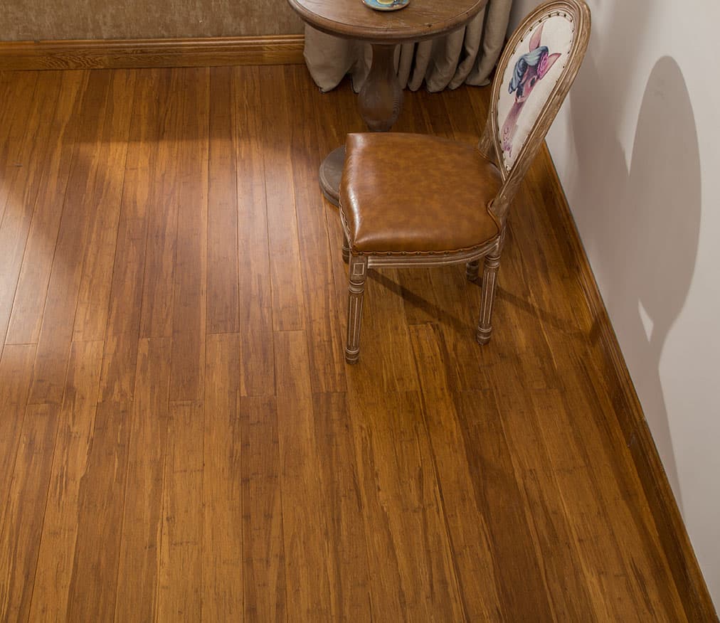
What Sets Bamboo Plywood Apart
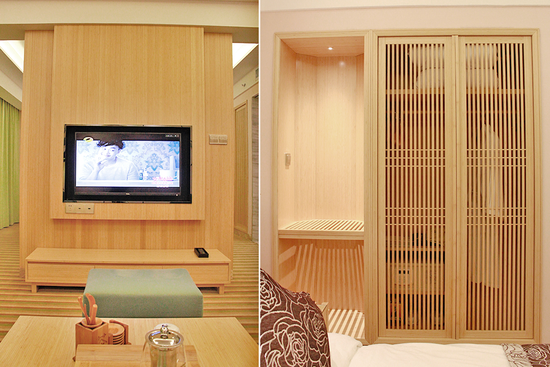
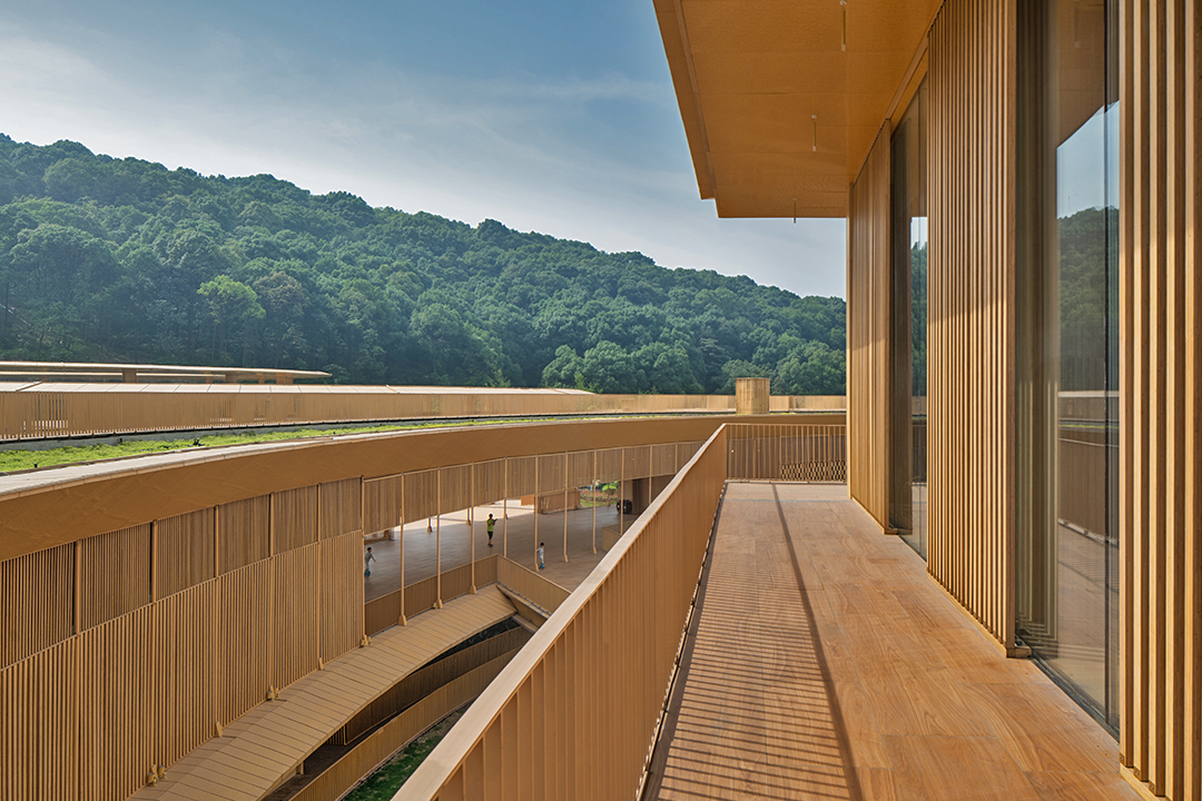
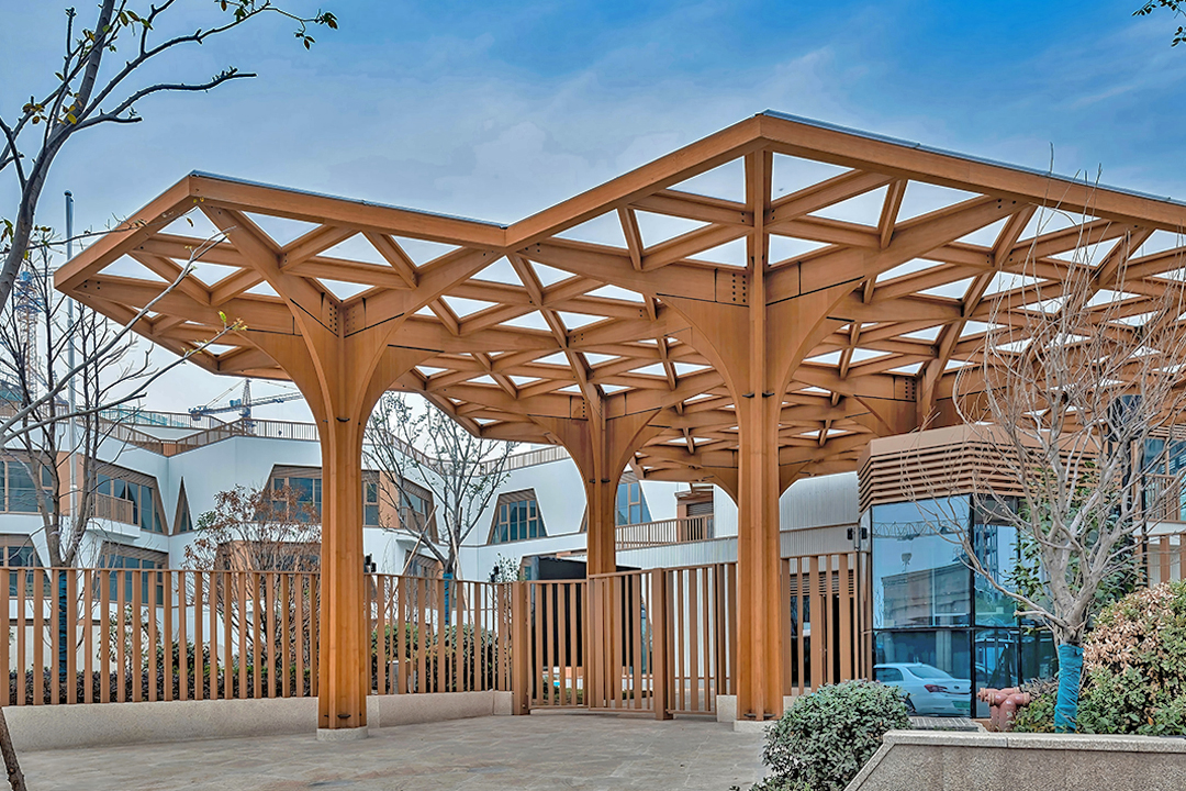
Bamboo plywood is created by laminating strips of bamboo into sheets. Vertical, horizontal, and strand‑woven constructions deliver different aesthetics and performance characteristics. Its natural linear grain gives it a distinct, modern appearance that appeals to architects and fabricators seeking alternatives to conventional hardwood plywood.
One of the defining qualities of bamboo plywood is its density. Strand‑woven types, in particular, are significantly harder than many hardwood species. This density contributes to a high level of structural integrity, making bamboo plywood a solid choice for applications where stiffness and resistance to wear are important.
Beyond strength, bamboo offers dimensional stability. Its laminated structure helps reduce warping, while its inherent tensile strength supports use in shelving, furniture frames, and cabinetry. Many appreciate that bamboo plywood provides the warmth and feel of wood without relying on slow‑growing hardwood trees.
How Traditional Plywood Performs
Traditional plywood consists of thin layers of wood veneers arranged in alternating grain directions and bonded with adhesives. This cross‑grain structure gives plywood its notable strength and ability to resist bending. Plywood has been a construction staple for decades because of its predictable performance and its ability to hold screws well.
Depending on the grade and species used, plywood can vary widely in appearance and cost. Higher‑grade sheets offer smoother surfaces and fewer voids, making them suitable for visible cabinetry and built‑ins. Lower‑grade versions are often used as structural substrates.
Moisture performance is one of plywood’s defining advantages. Exterior‑grade or marine‑grade options resist swelling and delamination better than MDF, making them suitable for kitchens, bathrooms, and certain outdoor or semi‑exposed applications. While bamboo plywood can outperform standard plywood in some moisture‑related conditions, marine‑grade plywood still holds a reputation for exceptional resilience when water exposure is likely.
Where MDF Fits Into the Comparison
MDF is produced by compressing wood fibers with resin under heat and pressure. Its fiber‑based structure creates a smooth, uniform surface free of knots or grain patterns. This consistent appearance makes MDF ideal for painted cabinetry, decorative millwork, shelving, and interior panels.
One of MDF’s biggest advantages is affordability. It often costs significantly less than bamboo plywood or hardwood plywood, making it a practical choice for budget‑focused projects.
However, MDF is not known for structural strength. While it is stable and easy to work with, it lacks the stiffness found in plywood or bamboo. This becomes evident in shelving or large spans, where MDF can sag under weight unless properly supported. Its screw‑holding strength is also lower, which can affect hardware installation and long‑term durability.
Moisture is another concern. Standard MDF absorbs water readily, leading to swelling or crumbling. Moisture‑resistant MDF options exist, but even these varieties do not match the performance of plywood or bamboo in wet environments.
Strength and Durability Comparison
A material’s ability to handle load, resist wear, and maintain its shape over time is crucial, especially in kitchens, custom furniture, and frequently used built‑ins.
Bamboo Plywood
Bamboo plywood generally offers superior strength compared with MDF and many traditional plywoods. Strand‑woven varieties approach or exceed the hardness of some hardwoods. This makes bamboo resistant to dents, scratches, and deformation.
Its laminated construction provides consistent dimensional stability. It holds fasteners well and performs reliably under repeated use. For heavily used cabinetry, desks, shelving, or tabletops, bamboo stands out as a robust option.
Traditional Plywood
Plywood’s alternating veneers give it excellent resistance to bending and warping. It performs well in structural roles and can handle moderate load applications without sagging. Screw‑holding strength is typically strong, especially in multi‑ply products.
Its durability depends on the wood species and adhesive quality. While not as dense as bamboo, many plywood types provide long service life in both interior and exterior applications.
MDF
MDF’s durability is closely tied to its intended use. It performs well in applications where the panel is supported on all sides, such as door panels or decorative trim. However, its ability to hold weight is limited, and it is more prone to dents and edge damage.
Once damaged, MDF is difficult to repair invisibly. Because of this, it is often chosen for painted surfaces where it will see minimal physical stress.
Surface Appearance and Finish Options
Aesthetic expectations often influence material selection just as much as performance.
Bamboo Plywood
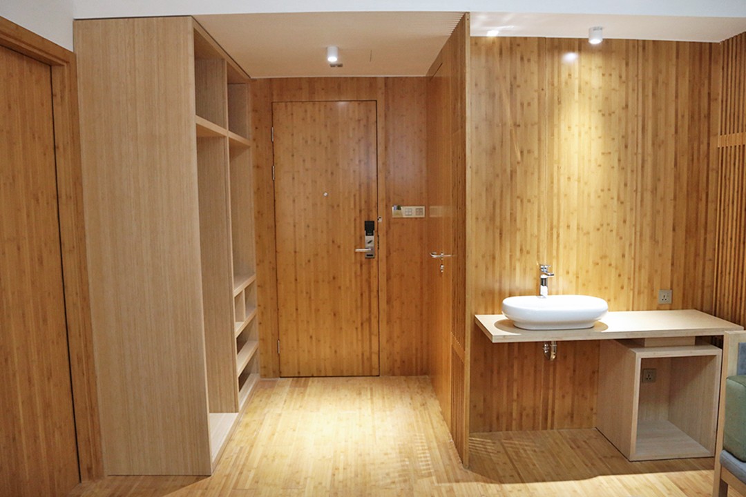
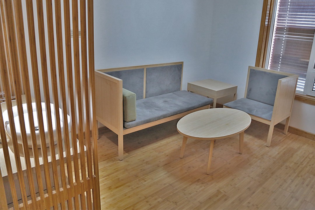
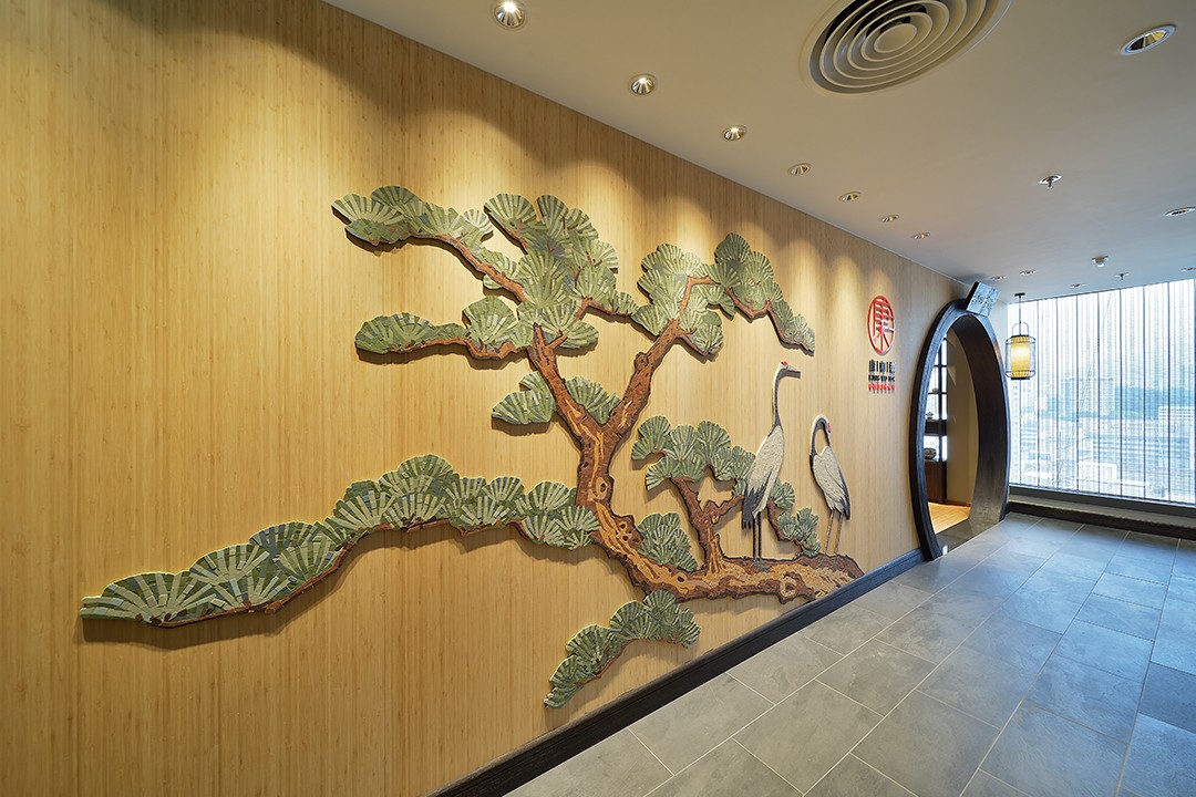
Bamboo’s natural grain brings a sleek, modern look. Vertical‑grain sheets offer a fine, linear aesthetic, while horizontal‑grain panels reveal wider bands and a more traditional appearance. Strand‑woven varieties highlight intricate patterns and natural variation.
It accepts stains, clear finishes, and oils well. Many prefer to highlight the natural appearance rather than paint it, though painting is possible with appropriate priming.
Traditional Plywood
Plywood’s appearance varies significantly depending on the species. Birch, maple, walnut, and oak plywoods are popular for cabinetry and fine furniture. Veneered plywood sheets offer attractive, natural wood patterns suitable for both clear coating and staining.
Because plywood includes real wood veneers, the surface can be repaired, sanded, and refinished, depending on veneer thickness.
MDF
MDF’s smooth, grain‑free surface is ideal for paint. It produces clean edges and takes routed profiles nicely, making it suitable for shaker‑style doors, trims, and panels. Because it lacks natural grain, it is rarely used with clear finishes or stains.
Workability and Fabrication
Ease of cutting, sanding, and joining influence how a project comes together, especially for custom builds.
Bamboo Plywood
Bamboo’s density can be both an advantage and a challenge. It machines cleanly with sharp tools but can dull blades more quickly than traditional plywood. Fastening is reliable, especially when pre‑drilling, and glued joints hold exceptionally well.
Fabricators appreciate that bamboo cuts without splintering when handled properly, making it suitable for precise joinery and exposed edges.
Traditional Plywood
Plywood offers predictable, easy handling. It cuts cleanly with quality blades and supports a wide range of joinery techniques. Lower‑grade plywood may chip more easily or have voids that complicate routing or exposed edges.
MDF
MDF is one of the easiest materials to machine. It cuts smoothly, sands evenly, and handles routing exceptionally well. However, the edges absorb paint more readily than the surface, requiring extra preparation. Dust during cutting is significant, so proper extraction is important.
Moisture and Environmental Performance
Moisture resistance can make or break a material choice for kitchens, bathrooms, laundry rooms, or humid climates.
Bamboo Plywood
Bamboo handles moderate moisture well, provided it is sealed properly. It is less prone to swelling than MDF and performs comparably to high‑quality plywood. While not designed for constant water exposure, it does well in controlled indoor environments.
Traditional Plywood
Plywood’s moisture performance depends on its grade. Exterior and marine grades offer excellent resistance, while interior grades are more susceptible to delamination if exposed to prolonged moisture.
MDF
Standard MDF performs poorly with moisture. Even moisture‑resistant MDF cannot withstand repeated or heavy water exposure. It is best reserved for low‑humidity environments.
Environmental and Sustainability Considerations
Sustainability plays a growing role in material selection, especially in cabinetry and interior architecture.
Bamboo Plywood
Bamboo’s rapid growth cycle and ability to regenerate from its root system give it strong environmental appeal. When sourced responsibly and produced with low‑VOC adhesives, bamboo plywood is considered one of the more eco‑conscious panel products.
Traditional Plywood
Sustainability varies widely depending on wood species, origin, and adhesive type. Many plywoods meet strong certification standards, but slow‑growing hardwood veneers raise concerns about long‑term resource availability.
MDF
MDF often uses wood byproducts and recycled fibers, which can reduce waste. However, resin content and the presence of formaldehyde‑based adhesives play a significant role in its environmental profile. Low‑VOC and no‑added‑formaldehyde MDF products are becoming more common.
Practical Applications and Where Each Material Excels
Each material has situations where it performs particularly well.
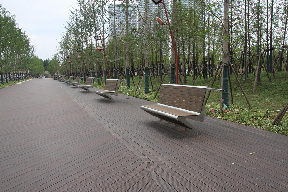
- Bamboo plywood is suited for cabinetry, countertops, shelving, furniture, wall panels, and architectural details where strength, appearance, and sustainability matter.
- Traditional plywood excels in structural applications, high‑load shelving, subflooring, built‑ins, and areas with potential moisture exposure.
- MDF works best for painted finishes, paneling, decorative trim, interior doors, and budget‑friendly cabinetry that avoids heavy load and moisture.
By matching materials to specific project demands, builders and designers can achieve strong performance and appealing visual results.
Final Thoughts
Bamboo plywood, MDF, and traditional plywood each offer unique advantages that make them suitable for different applications. Bamboo stands out for its strength, modern appearance, and sustainable nature. Traditional plywood continues to deliver reliable, versatile performance in both structural and finish roles. MDF remains a cost‑effective choice for smooth, painted surfaces and detailed interior work.
Understanding how these materials compare in durability, aesthetics, moisture behavior, workability, and environmental impact helps guide informed decisions for projects ranging from custom cabinetry to full interior remodels. Each has its place; the key is choosing the panel product that aligns with the project’s demands, style goals, and long‑term priorities.